chun@dronepcbworks.com · +86 769 8888 6666 · Mon-Sat 08:30-18:00 (GMT+8)
首页服务产品中心Gerber 预览报价关于我们
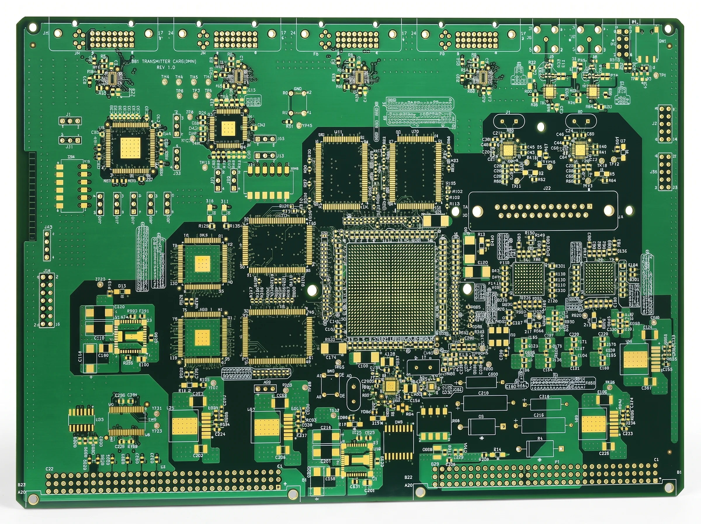
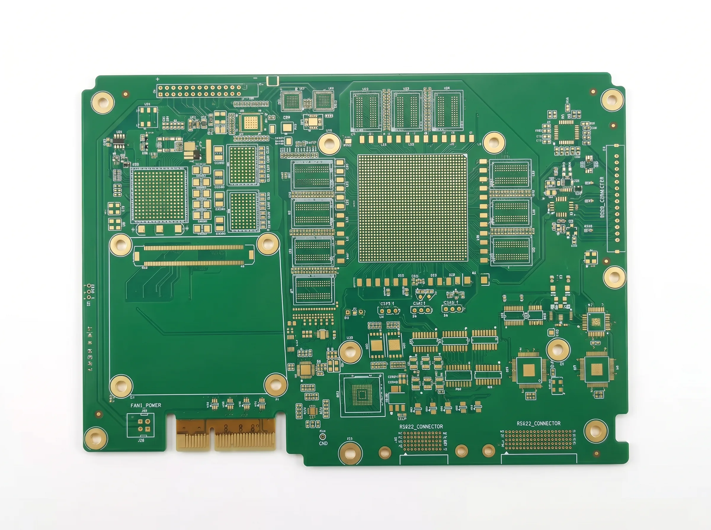
4 层飞控 PCB 点击放大
4 层飞控 PCB 4 层飞控 PCB 4 层飞控 PCB 4 层飞控 PCB 4 层飞控 PCB

描述

为飞控场景而做的叠层设计

飞控板工作在强振动、大电流、射频密集的环境里。这块 4 层板把电源层与敏感的模拟传感器层分开,并在 MCU 正下方铺完整地平面,使陀螺仪与气压计走线保持干净。

  • 叠层:信号 / 地 / 电源 / 信号,0.1 mm 半固化片
  • 差分对按 90 Ω ±5 % 走线,单端 50 Ω ±5 %
  • BGA 出线采用盘中孔,树脂塞孔并覆铜
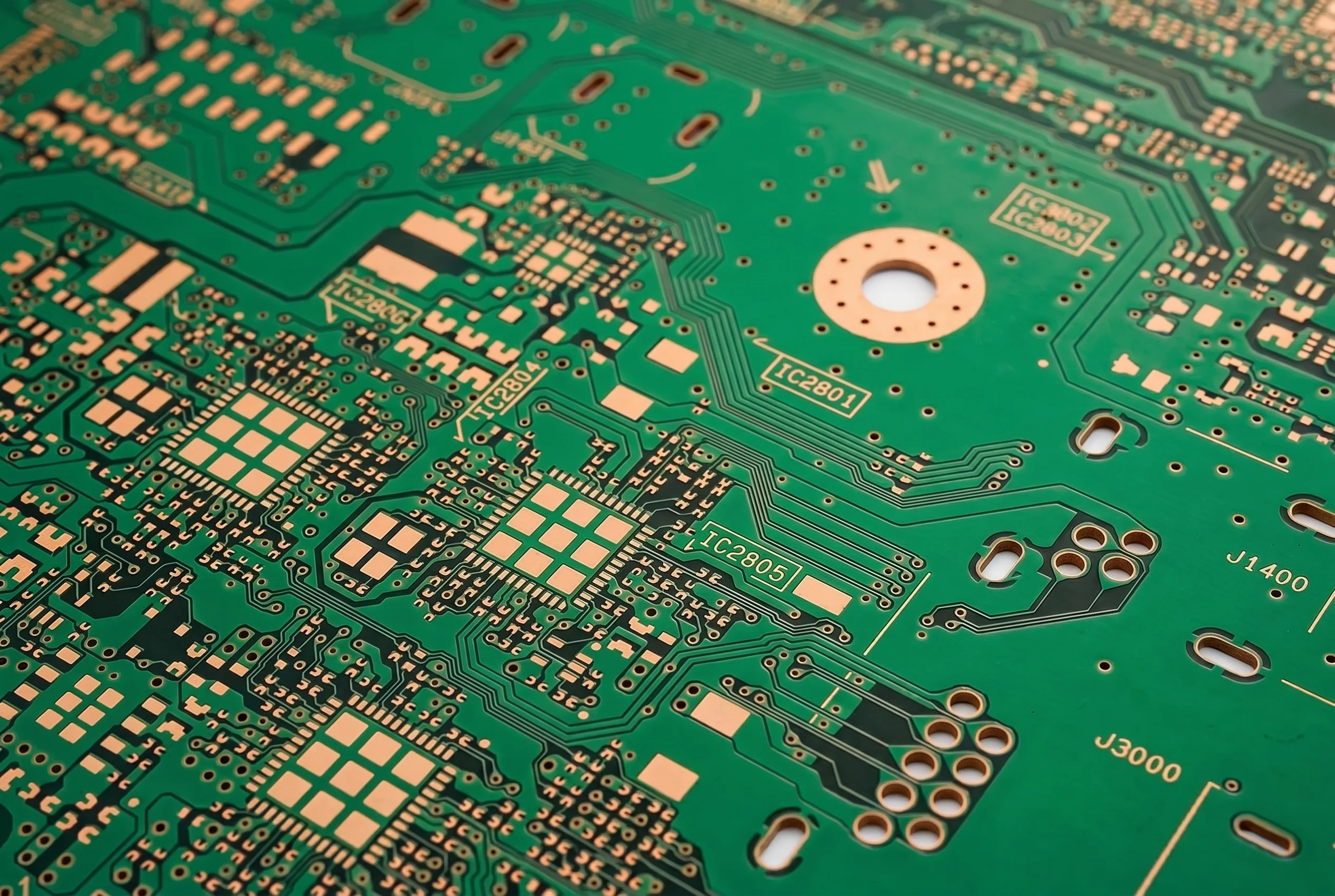
  • 哑黑阻焊 + 白色丝印,AOI 对比度更好
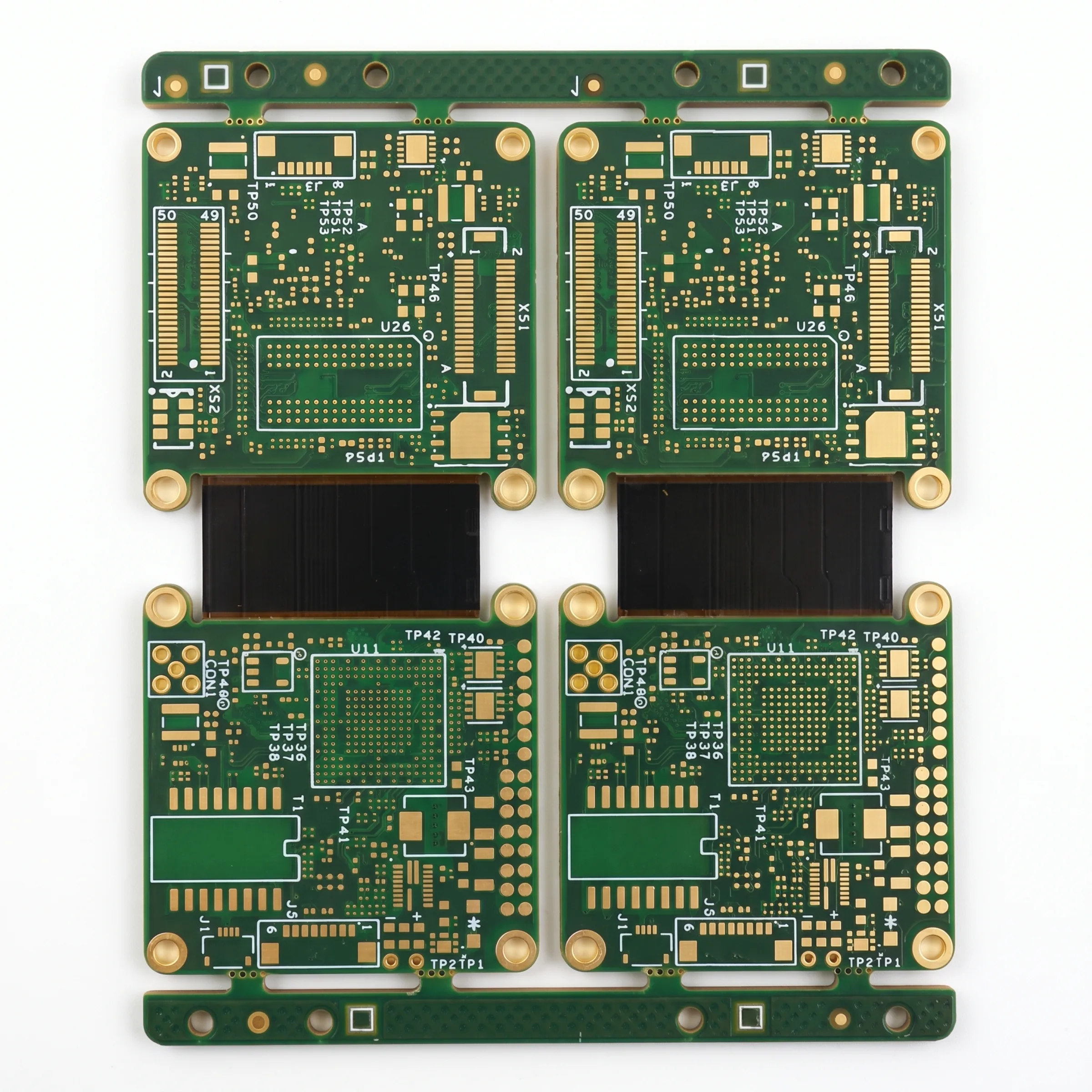
  • 拼板按 2 拼优化,小批量更省成本

下单说明

每块拼板都经过飞针电气测试,每个生产批次都会测量并记录阻抗测试条,检测报告随货发出。打样起订 5 片;500 片以上的批量可以重新拼板以提升材料利用率——请在询价单里注明预计年用量。

规格参数

层数4 Layers
基材FR-4 TG170
板厚1.6 mm ±10 %
铜厚1 oz / 1 oz
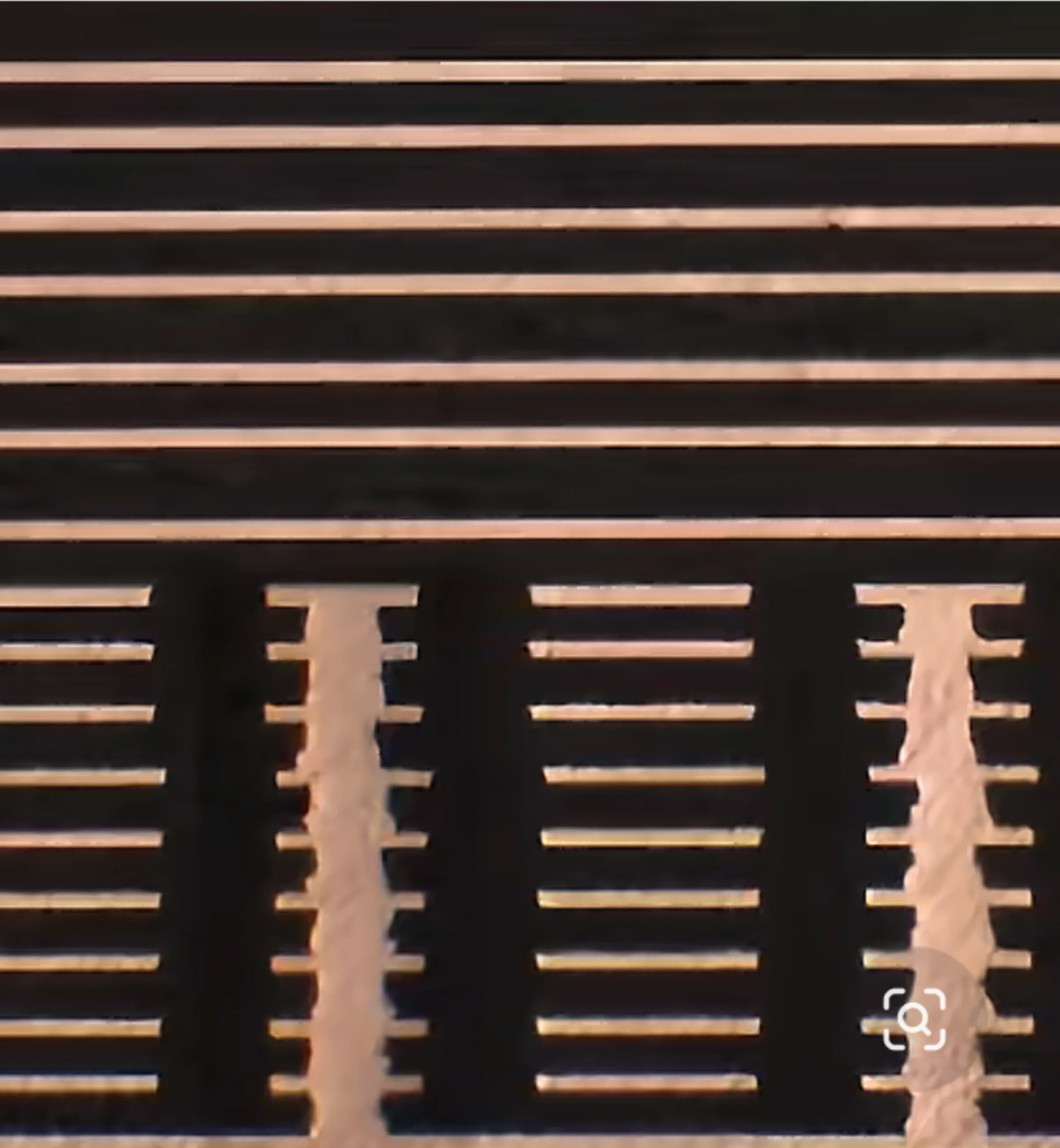
最小线宽线距0.09 / 0.09 mm
表面处理ENIG (Immersion Gold)
最小孔径0.20 mm
阻抗公差±5 %

DFM 指南

  • 最小线宽/间距 0.09 mm;叠层允许时建议留 0.10 mm
  • 环宽 ≥ 0.15 mm;盘中孔必须树脂塞孔并覆铜
  • 差分对 90 Ω ±5 %,单端 50 Ω ±5 %;有叠层文件请一并提供
  • 丝印线宽 ≥ 0.15 mm,与焊盘保持 0.20 mm 间距
  • 拼板间距 ≥ 1.6 mm;2 拼板加 3 个基准点 + 2 个工装孔
  • 批量生产每块拼板需带阻抗测试条

采购须知

Can I order a bare board instead of a fully assembled board?

Yes. The same Gerber and stack-up review applies; we fabricate the board only on Dongguan-managed lines, with no component sourcing and no SMT.

What do you need to send us?

Gerber files plus a one-line note on quantity, layer count, thickness and surface finish. BOM and pick-and-place files are only needed if you also want assembly.

How fast is a prototype?

2-8 layer prototypes typically ship in about 48 hours after the files are confirmed; small batches run from 5 pcs to 5,000 pcs on the same QC checklist.

Which tests are done before shipping?

AOI on the bare board, plus FAI and X-ray where assembly is involved. Every order is inspected against the same ZiLian checklist.

获取报价